During the opening keynote at the Intel Innovation event in San Jose, CEO Pat Gelsinger revealed a host of details about the upcoming Meteor Lake client platform. Intel’s Meteor Lake marks the beginning of a new era for the chipmaker, as it moves away from Intel’s messy 7 node and begins rolling out its own Foveros 3D packaging with EUV lithography for its upcoming customer mobile platform. Meteor Lake uses a tiled, disaggregated chip architecture for its consumer-focused processors for the first time, changing the nature of Intel’s consumer chips going forward. According to Intel, all of these changes have allowed them to make some significant advances in the mobile market.
Intel’s first chipset-based consumer CPU divides the common functions of a modern CPU into four individual boxes: compute, graphics, SOC, and I/O board. Within the compute board’s composition is a new pair of cores, a P core called Redwood Cove and a new E core called Crestmont. Both cores promise IPC gains over their previous counterparts, but perhaps the most interesting inclusion is a new type of electronic core built directly into the SoC board, which Intel calls a “low power island.” These new LP E cores are designed with the idea that light workloads and operations can be removed from the most power-hungry compute tiles and offloaded to more efficient, lower-power tiles altogether. Other key additions include Intel’s first-ever Neural Processing Unit (NPU), which is housed within the SoC and is designed to provide on-chip AI capabilities for inference and workloads, paving the way for the future.
With Meteor Lake, Intel aims to position itself more competitively in the mobile market, with notable improvements to the core compute hierarchy, Intel’s Xe-LPG Arc-based graphics board that looks to enhance integrated graphics capabilities, and an NPU that adds many One of the advantages is the advantages of artificial intelligence. Meteor Lake also sets the scene for Intel and modular disassembly, with Foveros 3D packaging set to become a mainstay of Intel’s processor roadmap for the future, with the Intel 4 process debuting and serving as a launching point for what will become Intel’s next mainstay of nodes throughout its factories, Intel 3.
Intel Meteor Lake: Intel 4 using Foveros 3D encapsulation
Intel’s Meteor Lake architecture is not just another iteration in a long line of processor developments; According to the company, it is a revolutionary leap forward. At the 2023 Intel Technology Tour in Penang, Malaysia, Michelle Johnston Holhaus, executive vice president and general manager of Intel’s Customer Computing Group (CCG), eloquently noted that Intel has reached an inflection point in its customer roadmap. Revealing more details about Meteor Lake at Intel’s technology tour in Malaysia, the architecture is a step up from existing customer processors in terms of performance as we progress through Intel’s “5 nodes in 4 years” roadmap.
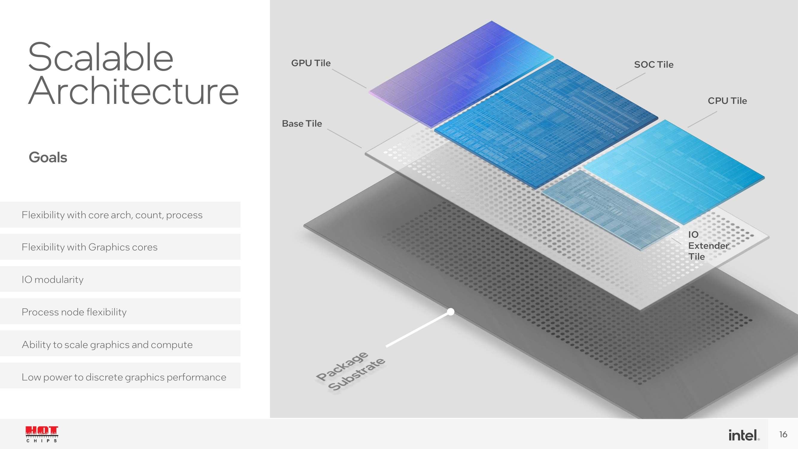
Meteor Lake is built on Intel’s detailed architecture pushed through Foveros packages. This is designed to improve performance and energy efficiency. The architecture itself consists of four unique and distinct tiles connected via Intel’s Foveros 3D packaging technology. This includes the compute board, which is built on Intel 4, while the graphics board is built on TSMC’s N5 node. The other two tiles that Intel is implementing within Meteor Lake are SoC tiles that act as a central hub through the embedded NOC. This is the first time Intel has used Network-on-Chip (NOC) technology on its customer processors, a simplified approach to NOC on its existing Agilex FPGAs. While in Agilex, the NoC is allocated to different NoC targets and switching takes place within the NoC infrastructure, in Meteor Lake, it connects directly to the I/O fabric through the IoC, which then moves to the I/O fabric. The NoC itself is directly connected to the graphics tiles, compute tiles, and other components within the SoC.
This modular approach allows for a comprehensive and scalable power management architecture that supports segmentation, allowing each slab to operate independently. This partitioned design prioritizes performance by eliminating bandwidth bottlenecks through things like I/O in a monolithic design and targets improved power efficiency. Perhaps the most notable element of the classification is that Intel can define specific silicon processes for each tile and is not limited to a single process node. On top of the power efficiency and package space benefits of tiled architecture, it is cheaper for Intel to manufacture CPUs with fewer masks through EUV, but it allows Intel to extend new IP to future products while maintaining the same base, which is another cost saving factor (for Intel ).
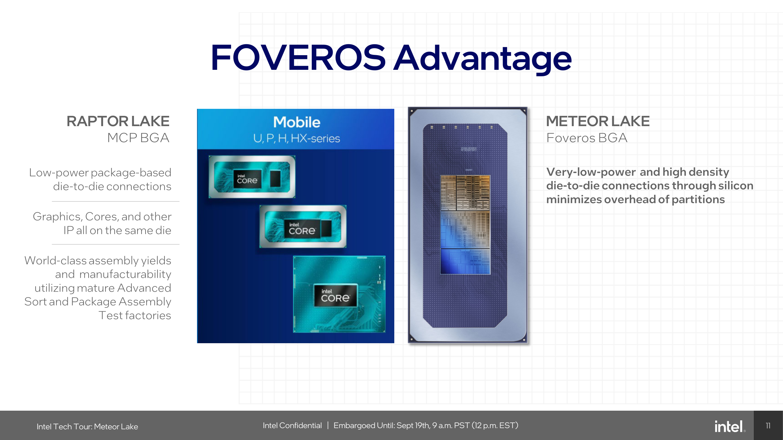
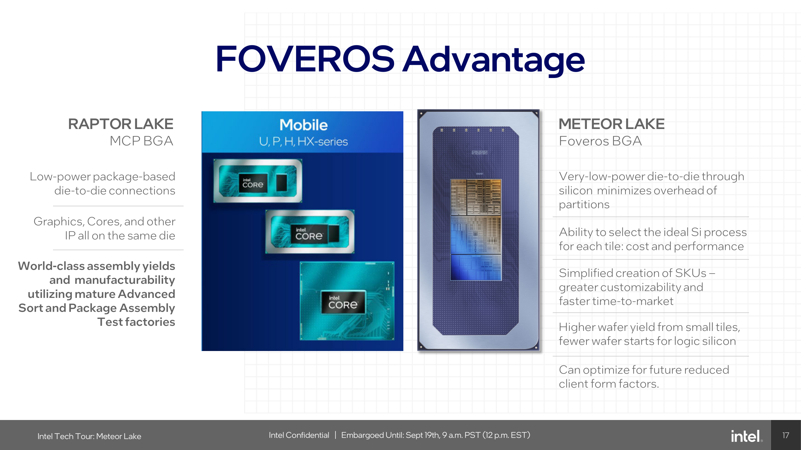
Compared to the portable Raptor Lake, which is made using multi-chip packaging (MCP), Meteor Lake uses Foveros BGA packaging and provides low-power interconnects, which Intel has confirmed have a small power penalty of between 0.15 and 0.3 picojoules. (pJ) Tile-to-tile communication. Some of the advantages of Foveros include better customizability through tiling, allowing Intel to manufacture chips and implement specific tiles and IP depending on chip grade, etc., low power with more I/O operations, or high-end tiles with all the latest gadgets and gizmos . Since the Intel 7 node is not as viable as they had hoped, Intel is promising higher throughput of chips on the Intel 4, which uses less chip space for logic-based silicon.
Power is managed using a scalable power management system that supports independent performance of each tile. Coordination between multiple Power Management Controllers (PMC) and system software is designed to optimize different workloads. Intel’s Meteor Lake architecture also introduces a new scalable fabric to improve power efficiency and expand bandwidth in previously bottlenecked areas, such as I/O.
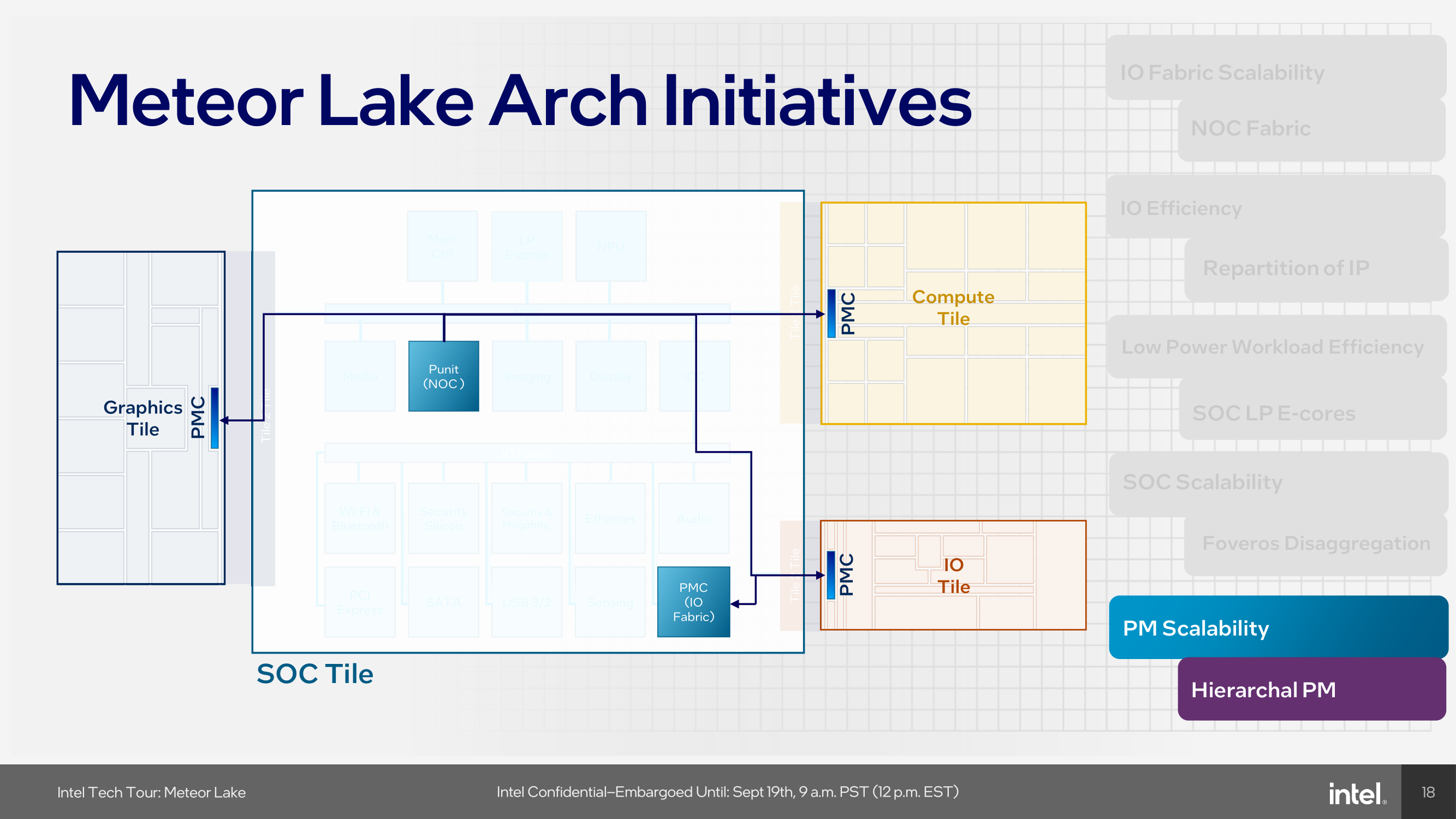
Moving further into the power controllers within the Meteor Lake architecture, Intel has integrated independent power management controllers within each board. As part of the breakdown of using Foveros, each tile must be managed independently for power, and using PMCs in the NoC, the I/O fabric, as well as each tile allows power to be managed independently depending on the number of cores on each stack.
Meteor Lake itself represents a massive architectural shift, not just an incremental update, as it represents the most significant architectural shift in client processors in four decades. This is because it is the first client processor to be manufactured using microchips instead of a monolithic design. The architecture is designed to be a cornerstone of Intel’s strategy to drive PC innovation for the next decade. Looking at some of the nitty-gritty of Intel’s Meteor Lake architecture, it uses Intel’s Foveros packaging technology, which uses 3D chip stacking to address the pitfalls of traditional 2D chip layouts.
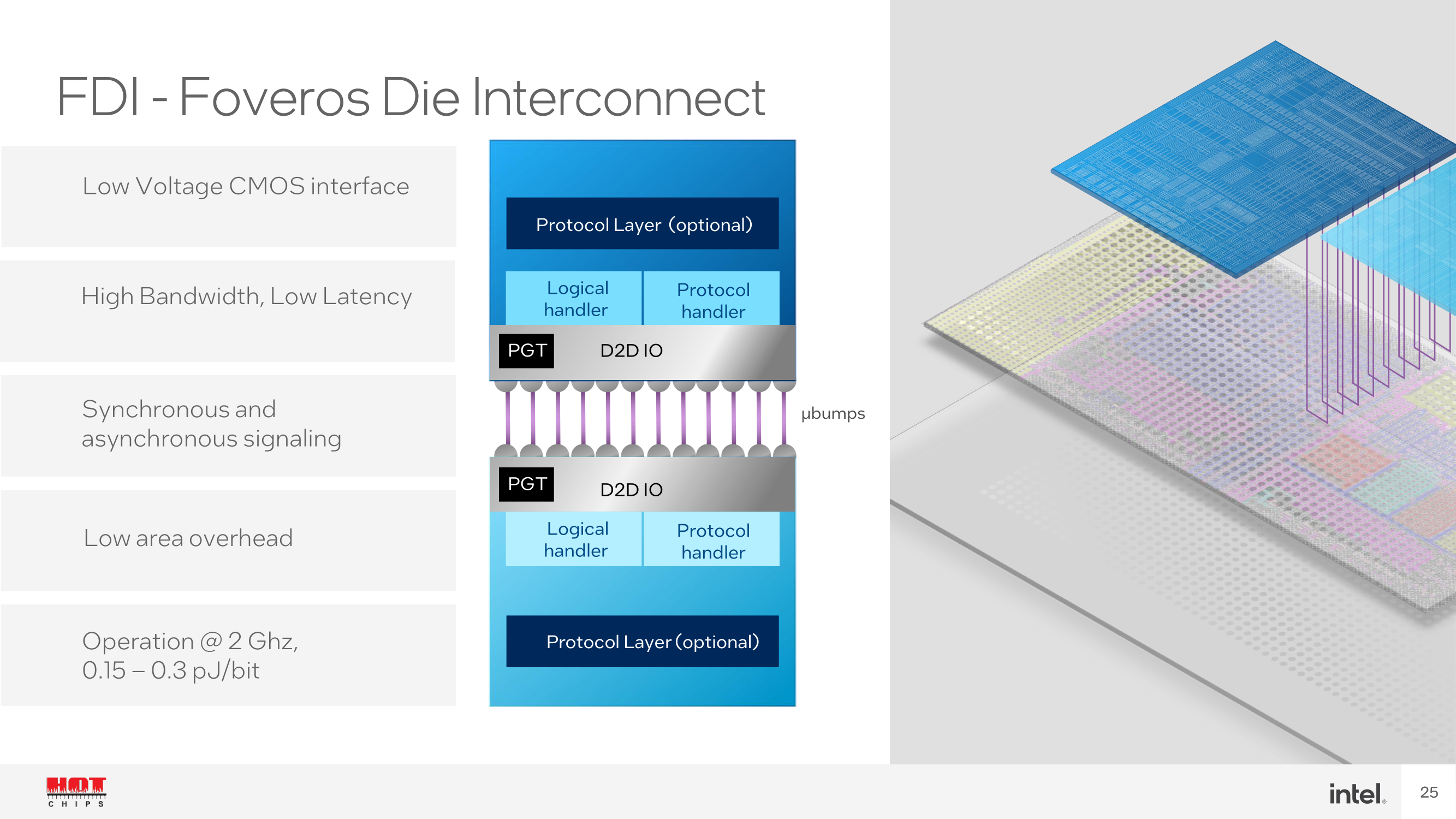
As we can see from Intel’s reveal above at Hot Chips 2023, the top and bottom layers have protrusions to connect each die together. The use of Foveros FDI packaging provides an interface to low-voltage complementary metal oxide semiconductor (CMOS), meaning that the power circuits can be operated at lower voltages and, therefore, with a lower power envelope. Another benefit of FDI is synchronous and asynchronous signaling, which means that signal transmission can handle fully duplex data blocks.
Creating the Meteor Lake SoC involves a substrate package, the foundation on which the tiles are placed, which uses the Foveros Die Interconnect (FDI). The core tile has a 36 µm die with metal layers and an actuation energy of 0.15 to 0.3 pJ at 2 GHz; This may fluctuate or vary depending on voltage, amps and frequency. Because it is a basic tile it is not Active chip itselfIts sole function is to serve as a base for all the different logic and metal layers of the chips to be placed.
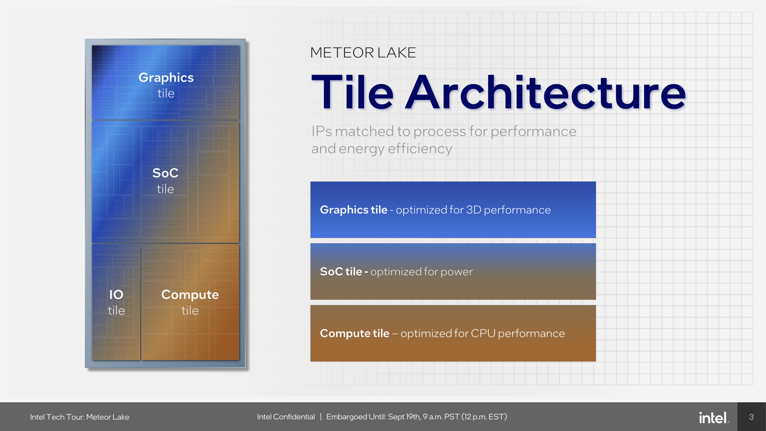
Intel’s Meteor Lake architecture architecture uses four distinct boxes to create a Meteor Lake CPU. This includes the Compute board, SoC, GPU, and I/O board, all of which have distinct uses, capabilities, and flexibility in relation to IP. Energy management is also getting a revamp. And with Intel’s Foveros packaging technology, each tile in Meteor Lake requires its own power management. Intel’s solution is a hierarchical power management system that uses power management controllers on the NoC and IO fabric and each individual board.
Over the next few pages, we’ll provide insight into each of the four squares, what each square brings to the table, and more about the various technologies driving innovation across Meteor Lake.

“Typical beer trailblazer. Hipster-friendly web buff. Certified alcohol fanatic. Internetaholic. Infuriatingly humble zombie lover.”